Designed Connectivity
If while traveling on the subway in New York City, one paused to consider how complex such a system is, one’s mind could not fully appreciate all the accomplishments that needed to take place in unison to deliver such a solution. It starts with the busy streets, bordered by sidewalks that lead to stairs. Stairs lead down to stations located at different depths. Stations house trains, passing through so quickly they appear as a blur, day and night without mishap. What brings all the layers of transportation togethers are the stairs. Without the stairs, the sidewalks and stations would not be connected, preventing the passengers from riding the trains.
The same can be said about drilled holes used on a printed circuit board. Without holes, the electrical connection between the layers of copper would not exist, deeming the board useless. Without the holes, there would be no way to affix the board to an enclosure. Drill holes connect the copper layers like stairs connect the different levels within the city. In the world of ODB++Design this information is housed in a simple and elegant manner.
Plated Through Hole (PTH) and Non-Plated Through in PCB design
ODB++D begins with classifying holes as either plated (electrical) or non-plated (non-electrical). A plated hole can also be a via (electrical). Plated and via holes are electrically the same, their hole walls have been plated in a similar fashion to how silverware is plated. The difference between a plated hole and vias is simple, a via is simply an interconnect between layers, where a plated hole will also have a component wire or pin, or even a mechanical screw placed through the hole. The wires and leads are later wave soldered, electrically connecting the component wire or pin to the printed circuit board.
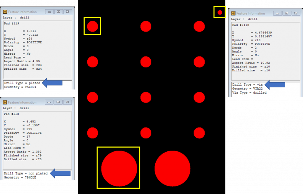
Finished hole sizes in PCBs
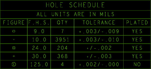
To complicate matters, EDA solutions work based solely on defining the finished hole sizes and do not take into consideration that the actual drills sizes will need to be larger to allow for the plating of the hole walls which will reduce the hole size back to the finish hole size. The finished hole sizes are historically communicated using a drill chart located on a drawing whose values are then manually entered to determine the necessary drill size.
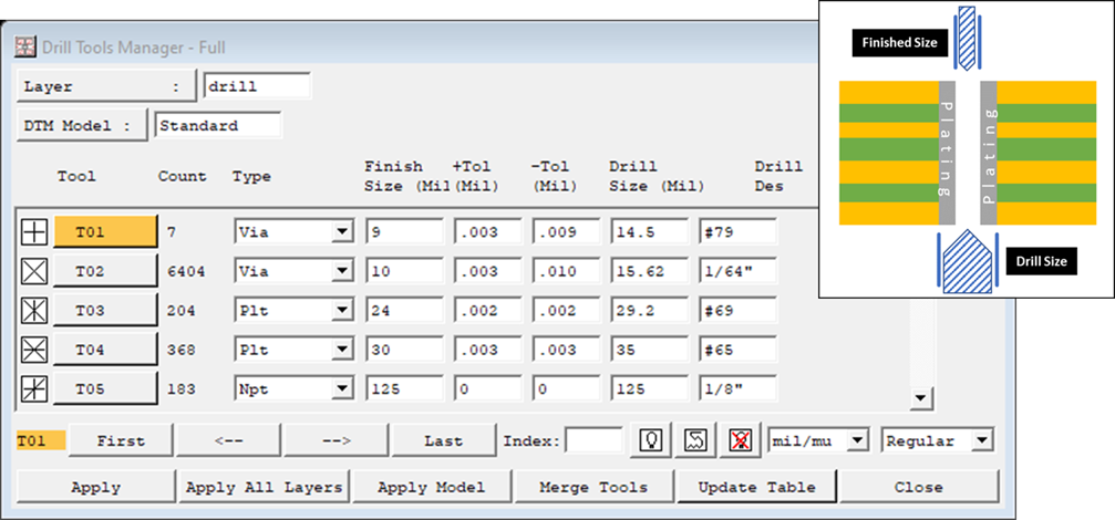
To facilitate the combination of finished size and the calculated drill size the ODB++D format has an entire table which is expanded to include tolerances and the drill designator located on a machinist drill table.
PCB hole depth
Currently, we have the three hole types and up to two holes sizes that need to be properly modeled to support a printed circuit board for DFM analysis and manufacturing. The next measurement we need is the depth, or layers, the drill holes penetrate. In most cases, holes will go entirely through the printed circuit board. These are simply referred to as through holes. Then there are blind holes. These start from the outside and end within the printed circuit board. Next are buried holes that through an additional manufacturing process begin and end within the printed circuit board. There’s an even greater variety of hole types, such as backdrill, counter bore, and countersunk to name a few. Those types will be expanded on in another article.
Through holes, blind holes and buried holes
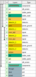
ODB++D enables through, blind and buried holes through a simple matrix implementation where each drill layer is accompanied by a start and end layer.
The ODB++D format is elegantly designed for fast and reliable transfer of a printed circuit board design requirement leading directly into manufacturing. The format is designed in such a fashion that applications can quickly identify the portions of the ODB++ that are relevant their needs leading to faster development times and prompt application behavior.
Read more about ODB++Design in our Resources section.
